Common emitter transistor amplifier theory of relativity Circuit Diagram There are different types of transistor amplifiers operated by using an AC signal input. This is interchanged between the positive value and negative value, hence this is the one way of presenting the common emitter amplifier circuit to function between two peak values. This process is known as the biasing amplifier and it is an important amplifier design to establish the exact operating point A 0.05 volt signal in the input circuit (emitter-to- base in Q 1) has controlled a 2.5 volt signal in the output (emitter-to-collector in Q 1). This is amplification. Figure 3. Relationship of an output signal and ac signal across R 1. You May Also Read: Transistor as an Amplifier: Working & Circuit | NPN Transistor Amplifier; Computing Gain
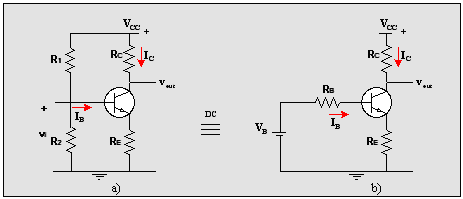
The single stage common emitter amplifier circuit shown above uses what is commonly called "Voltage Divider Biasing". This type of biasing arrangement uses two resistors as a potential divider network across the supply with their center point supplying the required Base bias voltage to the transistor. Key learnings: Common Emitter Amplifier Definition: A common emitter amplifier is a transistor configuration where the emitter is grounded, and the input signal is applied to the base.; Working Principle: In a common emitter amplifier, a small change in the base current causes a large change in the collector current, amplifying the input signal.; Phase Shift: The amplifier causes a 180-degree
Common Emitter Amplifier Circuit: Explained with Formulas Circuit Diagram
Transistor amplifiers are used frequently in RF (radio frequency), OFC (optic fibre communication), audio amplification, etc. In this lesson, we will discuss how a transistor works as an amplifier. Common-Emitter Configuration. For a transistor to work as an amplifier, we usually use the common-emitter configuration. In Common Emitter configuration, emitter terminal is taken as common for both input and output. So input is given between base and the emitter terminals and output is taken between collector and emitter terminals. This is the most commonly used configuration. Circuit diagram of Common Emitter NPN and PNP Transistor:

In this case if we applied the input signal of 0 degree phase then output will be obesrved to be Phase of 180 degree. The common-emitter amplifier design is called an inverting amplifier. Examples. Q1. The output resistance of a common base transistor amplifier is 100 kΩ, while the input resistance is 10 Ω. One kΩ is the collector load.
Common Emitter Amplifier: Working & Circuit Diagram
Now to make sure that the transistor can work properly between these two extreme points, we need to set things up in a specific way. This setup is often called "presetting" and it usually involves using a common emitter amplifier circuit configuration. To make this all work smoothly, we use something known as the "biasing".
To make them work for amplifying AC signals, the input signal must be offset with a DC voltage to keep the transistor in its active mode throughout the entire cycle of the wave. The current gain of a common-emitter transistor amplifier with the load connected in series with the collector is equal to β. The voltage gain of a common-emitter